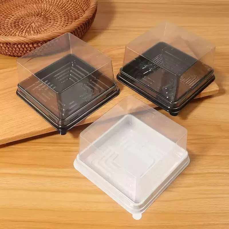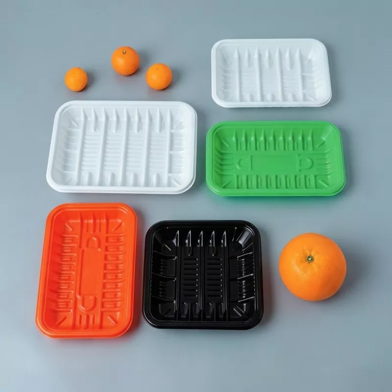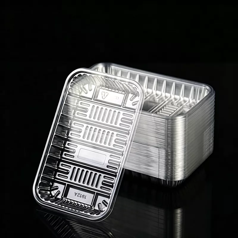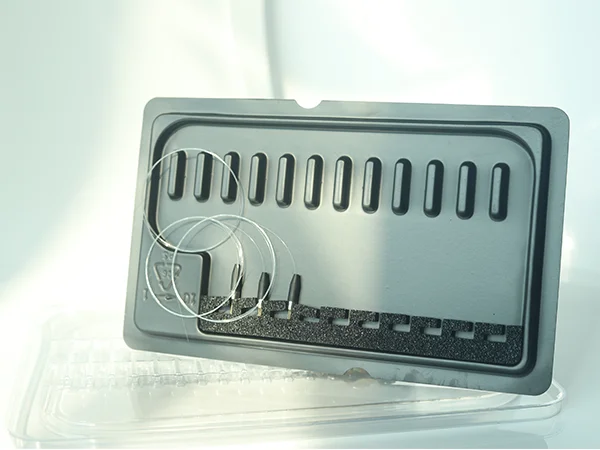

Static electricity is a practical concern in electronics manufacturing because sensitive components can be exposed to electrostatic charge during storage, handling, assembly, inspection and transportation. Packaging therefore needs to do more than separate products physically. It should also provide controlled electrostatic behavior while maintaining the dimensional, mechanical and cleanliness characteristics required by the application. Thermoformed trays made from PP, PET, PS and other suitable plastics can be configured around individual components, circuit boards, connectors, sensors, optoelectronic parts and industrial electronic assemblies. The material, surface resistance range, cavity geometry, wall thickness, color, surface treatment and stacking structure can all influence how the finished packaging performs. A well-designed Anti-Static Thermoplastic Packaging begins with the component and handling environment, then connects material selection with cavity layout and production controls. Large-format thermoforming also makes it possible to develop packaging for oversized components or multi-part systems rather than limiting the solution to small standard trays.
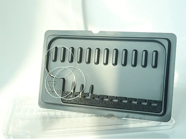
Table of Contents
Click any section below to jump directly to the topic you want to explore.
- 01. What Does ESD Packaging Need to Control?
- 02. Which Thermoplastics Fit Different ESD Applications?
- 03. How Should Surface Resistance Be Specified?
- 04. How Should an ESD Tray Be Designed?
- 05. Why Is Thermoforming Useful for Electronic Trays?
- 06. Where Are ESD Trays Commonly Used?
- 07. How Do Cleanliness and Product Protection Work Together?
- 08. What Information Is Needed for Custom Development?
- 09. What Should Be Checked Before Shipment?
- 10. Frequently Asked Questions
What Does ESD Packaging Need to Control?
Electronics packaging serves as part of the handling system around a component. When that component is sensitive to electrostatic events, the tray must provide predictable electrical behavior in addition to physical organization. This is why ESD packaging should be specified through measurable material and surface characteristics rather than through appearance alone.
Static charge can develop through contact and separation between different materials, movement during handling, friction and other common manufacturing activities. A sensitive component may pass through many stages before final assembly, so the packaging may be opened, transferred, stacked and reused several times. Each stage creates opportunities for uncontrolled electrostatic conditions if the packaging has not been designed appropriately.
The packaging structure also influences product movement. A tray with dedicated cavities can keep individual components separated and reduce unnecessary contact between neighboring parts. For connectors, sensors, PCB-related components and other precision products, controlled positioning can make manual and production-line handling more orderly.
Electrostatic Behavior
The material should provide a defined surface resistance characteristic appropriate for the intended ESD protection strategy. Different products and handling environments may require different electrical properties.
Mechanical Protection
The tray should physically support the part and reduce unwanted movement, contact and impact during normal storage, transfer and transport operations.
Dimensional Organization
Product-specific cavities keep components in controlled locations and can make loading, unloading, inspection and production-line transfer more predictable.
Handling Compatibility
The tray should be designed around the actual process, including manual handling, automated movement, stacking, nesting, temporary storage and line-side turnover.
Effective electronic packaging combines electrostatic control with physical organization. Neither function should be treated as an isolated feature.
It is also important to understand that not every electronic component has the same sensitivity or handling requirement. Semiconductor packages, connectors, sensors, optical modules and assembled circuit boards can differ in weight, shape, exposed surfaces and process environment. Packaging should therefore be developed around the actual product rather than relying on one universal tray structure.
- Defined ESD behavior: the electrical characteristics should be specified according to the component and process requirements.
- Stable positioning: individual cavities can limit unwanted movement during handling.
- Appropriate structure: wall thickness, depth and geometry should match the physical product.
- Process compatibility: stacking, nesting, inspection and line-side handling should be considered from the beginning.
Which Thermoplastics Fit Different ESD Applications?
Thermoplastic selection affects more than electrical behavior. It also determines rigidity, impact resistance, flexibility, transparency, temperature behavior, appearance and forming characteristics. For electronic trays, these properties need to be considered together because a material that provides one desirable feature may introduce limitations in another area.
PP for Repeated Handling
PP is useful when a tray needs a combination of flexural fatigue resistance, drop resistance and temperature resistance. These characteristics are relevant in applications where the tray may be repeatedly loaded, transferred, stacked or returned to a production area.
SMT environments can involve frequent handling and organized movement between process stages. A PP-based structure may be considered where the packaging must tolerate repeated use while maintaining its defined electrostatic characteristics.
PET for Transparency and Rigidity
PET provides high transparency and good hardness, making it useful where component inspection and product visibility are important. A transparent tray can make it easier for operators to identify the component arrangement without removing each item from its position.
Visibility can also support inspection-oriented workflows. When the packaging concept allows operators to see the product directly, the tray can provide organization while preserving a clear view of the component.
PS for General Tray Structures
PS is relatively brittle and has somewhat lower transparency than PET. It can nevertheless be considered for general-purpose electronic component turnover trays where the overall structure and handling environment are compatible with its characteristics.
The correct choice should not be based on a material name alone. The actual component weight, cavity dimensions, expected impact, temperature conditions, transparency requirement and intended handling frequency all influence the selection.
| Material | Main Characteristics | Typical Applications | Key Selection Considerations |
|---|---|---|---|
| PP | Good flexural fatigue resistance, drop resistance and temperature resistance. | SMT handling trays, turnover trays and reusable electronic packaging. | Repeated handling, impact exposure, temperature conditions and structural flexibility. |
| PET | High transparency and good hardness. | Inspection trays and packaging where component visibility is important. | Transparency, rigidity, appearance and required cavity structure. |
| PS | Relatively brittle with slightly lower transparency. | General electronic component handling and turnover trays. | General structural requirements and handling conditions. |
| Other Suitable Thermoplastics | Selected according to specific product and process requirements. | Specialized customized electronic packaging. | Required electrical, mechanical, environmental and appearance characteristics. |
In practice, electrical performance should remain connected to mechanical performance. A tray may have the desired resistance range but still be poorly suited to the product if its shape, flexibility or temperature behavior does not match the handling environment.
How Should Surface Resistance Be Specified?
Surface resistance is one of the central technical parameters in ESD packaging because it provides a measurable way to describe the electrical behavior of the packaging material. The target range should be selected according to the component's ESD requirements and the surrounding handling environment.
A customized packaging program can specify surface resistance from 1.0×10⁴Ω to 1.0×10¹¹Ω. That range covers multiple electrostatic-control requirements, but the existence of a wide range does not mean that one value is automatically suitable for every application.
Different electronic manufacturing environments can have different requirements for charge control, material handling and process integration. A tray used for general component turnover may have a different specification from a tray used for sensitive inspection, automated handling or packaging of components with exposed conductive structures.
Start With the Component Requirement
The first question should be what level of ESD control is required by the component and handling process. The packaging specification should then be developed around that requirement rather than selecting an electrical value simply because it is commonly used.
Consider the Complete Packaging System
The tray is only one element of the packaging environment. Outer cartons, cushioning materials, separators, work surfaces, handling equipment and other packaging components can also influence the electrostatic conditions around the product.
This makes system-level thinking important. A tray with a controlled resistance characteristic should still be integrated into a handling process that recognizes the electrical behavior of the surrounding materials and equipment.
Connect Resistance With Geometry
Electrical specification should not cause engineers to overlook physical protection. The cavity depth, wall spacing and positioning structure need to protect the component while preserving the required electrostatic function.
- Define the required resistance range: connect the target value to the actual ESD protection requirement.
- Keep the component in a controlled position: use cavities and locating features where needed.
- Review the complete handling environment: consider the other materials and equipment that interact with the tray.
- Verify the finished product: use suitable resistance-testing equipment to check that the specified electrical characteristics are achieved.
A measurable specification also makes communication easier between packaging designers, component manufacturers and production teams. Instead of describing a tray only as “anti-static,” the project can identify the intended resistance range and the material construction required to achieve it.
How Should an ESD Tray Be Designed?
Electrical control is only part of the design problem. An electronic tray must also hold the component securely, allow practical loading and unloading, fit the handling equipment and remain compatible with stacking or nesting requirements.
1. Define the Product Envelope
Begin with the exact dimensions of the component. Record length, width, height, diameter, protrusions, connector locations, sensitive surfaces and any areas that should not make contact with the tray.
For irregular electronic assemblies, the useful design information may include several cross-sectional dimensions rather than one overall size. This can be especially important for connectors, sensors and PCB assemblies with protruding components.
2. Build the Cavity Around the Product
A dedicated cavity can control the position of each part while creating separation between neighboring components. Cavity geometry should balance retention and accessibility. Excessively loose positioning may allow movement, while overly restrictive geometry can make loading and unloading difficult.
3. Consider Wall Thickness
Wall thickness influences tray rigidity, weight and forming behavior. Large cavities and deep structures may require careful consideration of material distribution during thermoforming. Thickness should therefore be evaluated alongside the forming direction and final tray geometry.
4. Add Stacking or Nesting Features
Reusable electronic trays often need to be stacked when loaded and nested when empty. These features can reduce storage complexity and improve handling efficiency, but the geometry needs to be designed so stacked trays remain stable and the cavities do not interfere with one another.
5. Protect Sensitive Surfaces
Components may have exposed housings, connectors, lenses, pins or finished surfaces that require controlled contact. Where appropriate, the tray can be configured with protective inserts or selected cushioning features so the product is supported without unnecessary surface contact.
6. Plan for Automated Handling
Electronics factories may move trays manually, with carts, conveyors or automated handling equipment. The tray structure should be compatible with the intended process, including access points, stacking height, orientation and loading direction.
Geometry
Dimensions, cavities, depth, spacing, openings and tray perimeter should correspond with the component and package environment.
Electrical Specification
The required surface resistance range should be defined according to the ESD characteristics required for the specific application.
Handling
Loading, unloading, stacking, nesting, inspection and line-side movement should all be considered during design.
Protection
Contact areas, cushioning features and cavity shape can be adapted to reduce unwanted movement and physical contact.
The most reliable tray designs are therefore application-specific. They do not rely on a fixed cavity pattern when the product itself has a unique shape or a special handling requirement.
Why Is Thermoforming Useful for Electronic Trays?
Thermoforming is particularly useful when electronic packaging requires customized cavities, large surfaces, curved contours or broad tray dimensions. A heated thermoplastic sheet can be formed over tooling to create a product-specific structure without forcing every application into a small standard format.
This is important for electronics because component packaging can vary from small individual parts to larger assemblies and multi-part systems. One tray may need a grid of small cavities, while another may require deep pockets for larger assemblies.
Large-Format Capability
Thermoformed packaging can be produced at dimensions of up to approximately 1300 × 750 × 740 mm, subject to the actual tray structure and production requirements. This broad forming capability is useful when a packaging system covers a large assembly or multiple product zones.
Customized Cavity Layouts
Thermoforming allows the cavity pattern to be developed around the product arrangement. Individual cavities can be spaced according to component dimensions, and the overall tray footprint can be adapted to existing transport or storage structures.
Development Flexibility
Electronic products can change during development. Connector positions, housing dimensions, PCB configurations and accessory arrangements may all be revised. A flexible thermoforming approach can support selected development projects where customized tooling and broad-format structures are required.
Material Variety
PP, PET, PS and other suitable thermoplastics can be considered within the thermoforming process. This allows the electrical, mechanical and visual requirements of the tray to be evaluated together.
Integration With Packaging Features
The forming concept can incorporate positioning areas, stacking structures, openings and other functional details. Where additional surface protection is required, selected cushioning materials can also be integrated into the packaging design.
Thermoforming is most useful when the packaging geometry needs to follow the product closely rather than forcing a complex component into a generic tray format.
The manufacturing process should still be selected according to the product geometry, required electrical behavior, production quantity and overall packaging strategy. Thermoforming is a process option rather than a universal answer for every electronic packaging application.
Where Are ESD Trays Commonly Used?
ESD-controlled thermoformed trays can support many stages of electronics production and logistics. The exact structure depends on whether the packaging is intended for storage, inspection, production-line movement, turnover or transportation.
- Electronic components: connectors, sensors, PCB-related parts, semiconductor components and other static-sensitive products can be arranged in dedicated cavities.
- PCB handling: circuit boards and electronic assemblies can be supported during temporary storage, transfer and production-line movement.
- Precision electronic parts: individual cavities can help maintain organized positioning for components with defined handling requirements.
- SMT manufacturing: reusable turnover trays can support repeated movement between manufacturing stages where controlled electrostatic behavior is required.
- Optoelectronic components: packaging can be configured for optical communication and optoelectronic assemblies with specified ESD conditions.
- Industrial electronic equipment: large components and assemblies can be organized for storage, internal transport and controlled handling.
Component Inspection
Inspection-oriented packaging benefits from organized positioning and clear access to the component. When transparency is important, PET can be considered for structures that allow the operator to see the product while it remains inside the tray.
SMT and Production-Line Turnover
Production environments can involve repeated tray movement between process stages. PP may be considered where fatigue resistance, impact resistance and temperature behavior align with the requirements of repeated handling.
PCB and Assembly Handling
Circuit boards and assemblies can have larger dimensions and fragile mounted features. Tray cavities should therefore support the board without contacting components that are not designed to bear load.
Optoelectronic Packaging
Optical communication components can have sensitive surfaces and precise dimensions. Their packaging structure should account for component orientation, contact zones, separation and the required electrostatic properties.
How Do Cleanliness and Product Protection Work Together?
Electronics packaging is not only an ESD-control device. Cleanliness can also be important, particularly when components are exposed to dust, particles or surface contamination during manufacturing. Packaging design should therefore address both electrostatic behavior and the physical cleanliness of the tray.
A clean production environment can help control dust adhesion during tray manufacturing. Material handling, forming, trimming and storage should be managed consistently so the finished tray is suitable for the intended electronics application.
Control Contact Areas
Not every component surface should touch the packaging equally. Some products have finished cosmetic surfaces, exposed contacts, optical surfaces or sensitive protrusions. Cavity design can limit unnecessary contact and keep delicate areas away from structural edges.
Use Protective Inserts When Appropriate
Selected packaging designs can incorporate cushioning materials such as sponge where an additional soft contact layer is needed. This approach can help reduce surface contact and handling marks for products with higher appearance or contact sensitivity.
Maintain Clean Handling Practices
Packaging performance is influenced by what happens after production as well as during production. Clean storage, controlled loading practices and appropriate handling procedures can help preserve the intended condition of the tray before it reaches the component.
Consider Reuse
Reusable trays may pass through many cycles of handling. When reuse is part of the packaging system, the design should consider fatigue, repeated cleaning, stacking and repeated loading. PP can be useful in applications where those characteristics align with the required electrical and mechanical performance.
ISO-based quality management can provide a structured framework for process control, while applicable third-party testing can be used to assess relevant material or product characteristics according to customer requirements.
What Information Is Needed for Custom Development?
Customized trays work best when the packaging design starts with clear information about the product and the handling process. The more complete the input, the easier it is to determine cavity geometry, material direction, resistance range and overall tray structure.
- Define the product. Provide the product dimensions, overall shape, critical protrusions and any areas that should remain free from contact.
- Define the handling environment. Explain whether the tray is used for storage, manual transfer, production-line turnover, inspection, stacking or transportation.
- Define the ESD requirement. State the required surface resistance range or the applicable packaging requirement for the component.
- Define the tray dimensions. Provide the desired overall length, width, height and any restrictions imposed by transport containers or production equipment.
- Define cavity structure. Determine the number of cavities, cavity depth, spacing, orientation and product loading direction.
- Define additional functions. Identify stacking, nesting, cushioning, positioning features, openings, labels or logo requirements where applicable.
- Review the material direction. Compare PP, PET and PS against the electrical, mechanical, temperature and appearance requirements of the application.
Drawings and Dimensional Data
Engineering drawings can provide precise information about critical dimensions, tolerances and component interfaces. Dimensional specifications are also useful when the product has a relatively simple geometry.
Physical Product Information
A physical product can help clarify irregular shapes, actual contact surfaces, height transitions and protruding components that may be difficult to describe through basic dimensions alone. The goal is to understand the real package envelope before the cavity design is finalized.
Packaging Equipment and Logistics
The tray should also be designed around the way it will move through the factory. Container dimensions, stacking height, nesting depth, conveyor clearance and operator access can all affect the final shape.
A project specification should therefore describe the complete journey of the tray, from loading through storage and production-line transfer to its final packaging or transportation stage. This broader view helps prevent the cavity design from solving only one step of the process.
What Should Be Checked Before Shipment?
Finished electronic trays should be checked from both electrical and physical perspectives. A tray can meet the intended dimensions while failing to maintain the required resistance characteristic, just as it can meet the resistance range while having cavity or stacking issues.
| Quality Area | What to Check | Why It Matters |
|---|---|---|
| Surface resistance | Check the specified electrical resistance range with suitable testing equipment. | Confirms that the finished packaging follows the required ESD specification. |
| Dimensions | Verify tray length, width, height, cavity dimensions and critical spacing. | Supports proper component positioning and compatibility with the packaging system. |
| Form accuracy | Inspect cavity shape, corners, walls, openings and formed profiles. | Helps ensure consistent physical protection and loading performance. |
| Surface condition | Check visible defects, contamination and overall tray cleanliness. | Supports the requirements of precision electronics handling. |
| Stacking or nesting | Confirm that trays align correctly when stacked or nested. | Improves handling stability and storage compatibility. |
| Protective features | Verify cushioning areas, positioning structures and product-contact zones. | Helps reduce unwanted movement and contact with sensitive components. |
Electrical Verification
The specified surface resistance range can be checked with suitable resistance-testing equipment. Verification should be performed according to the applicable testing method and packaging requirement.
Dimensional Verification
Critical dimensions should be measured against the agreed design requirements. Particular attention should be given to cavity depth, cavity position, tray perimeter and any feature that interfaces directly with the component or external handling equipment.
Cleanliness Inspection
Finished trays should be inspected for visible contamination and material debris. This is especially relevant for electronics packaging where cleanliness can influence the handling environment.
Production Consistency
Quality management should cover material input, forming conditions, trimming, inspection and finished-product handling. A repeatable process is important because the tray's electrical and physical characteristics both need to remain consistent throughout production.
Where required, raw materials and finished products can also undergo applicable third-party testing. The precise testing scope should be established according to the customer's technical requirements and the intended electronics application.
For a broader view of customized thermoformed packaging capabilities, visit Anti-Static Thermoplastic Packaging and compare the required material, resistance range, tray structure and application conditions before finalizing the packaging specification.
Frequently Asked Questions
Q1. What surface resistance range can be specified?
Q2. Which material is suitable for an ESD tray?
Q3. Can the tray be designed for SMT handling?
Q4. What is the maximum thermoformed packaging size?
Q5. Can the cavity layout be customized for different components?
Q6. Can different tray colors be produced?
Q7. Can logos or identification marks be added?
Q8. Can stacking and nesting structures be integrated?
Q9. Can cushioning materials be added?
Q10. What information should be provided for a customized tray?
Build an ESD Tray Around the Actual Electronics Application
Electronic packaging becomes more reliable when the electrical requirement and physical structure are developed together. Surface resistance, material choice, cavity geometry, wall thickness, product positioning, cleanliness and handling conditions all contribute to the final packaging specification.
A clear project brief can include component dimensions, drawings, required resistance range, tray footprint, cavity layout, stacking requirements and production conditions. These details make it easier to develop a packaging structure that fits the actual electronics process instead of relying on a generic tray format.
For customized ESD thermoformed packaging requirements, learn more about Shunxin and contact us to discuss your electronics packaging requirements.
Final material, resistance, geometry and production specifications should be confirmed according to the component, handling process and applicable quality requirements.